
wafer back grinding services malaysia manufacturer Grasping strong production capability, advanced research strength and excellent service, Shanghai wafer back grinding services malaysia supplier create the value and bring values to all of customers.
 WhatsApp)
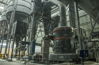
The LINTEC Adwill series includes UV curable dicing tapes, high performance back grinding tapes, dicing die bonding tapes required for semiconductor packaging, and backside coating tapes. Adwill continues to make steady progress in the advancement of related equipment and unique systems.
PDF | Ultrathin silicon wafer technology is reviewed in terms of the semiconductor applications, critical challenges, and wafer preassembly and assembly process technologies and their underlying ...
Wafer Services PVD and Dicing: Home Products Contact Assembly Wire Bonders Wafer PVD Vapor Deposition and wafer dicing services Available from these companies: Listed Alphabetically: Country: Address : Contact: PVD Coating Films: Back Grinding: Dicing: USA: American Dicing 7845 Maltlage Dr
Leadingedge CMP, wafer thinning and wafer polishing solutions.
In this process, a UVcurable adhesive is applied to wafer surfaces and used as a bonding agent between glass support substrates and wafers. Grinding stresses on the wafer are minimized as the adhesive flows into and supports the topography of the circuit patterns on the front side of the wafers.
Best Equipment for advanced DicingGrinding Service. DISCO''s highquality precision technology guarantees excellent processing results. Manufactured at the Kuwabata Plant in Hiroshima Prefecture, DISCO''s precision dicing saws and grinding/polishing machines, combined with etchers, surface planers and AOI tools, offer customers the highest level of quality.
WLP Services; Wafer Backside Metallization; Pac Tech offers high quality wafer back metallization process including back grinding and stress relief with TiNiAg qualified for PowerMOSFET and other devices. Ebeam evaporation technology. PacTech Asia uses an ebeam evaporation technology for its wafer backside metallization. ...
Syagrus Systems uses the 3M Wafer Support System to meet the demands of today''s technology companies for extremely thin silicon wafers and die used in complex applications. We have over 15 years of silicon wafer thinning and wafer backgrinding experience, including bumped wafer backgrinding and have provided wafer backgrind services since 1997. ...
Contacts page classic with contact form in HTML. grinding machine jobs in malaysia. We sincerely welcome you to contact us through hotlines and other instant communication ways.
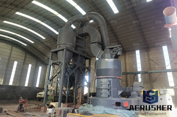
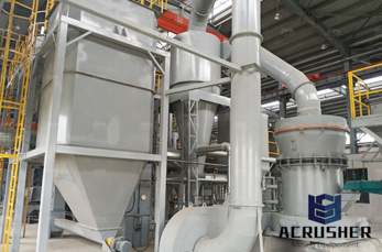
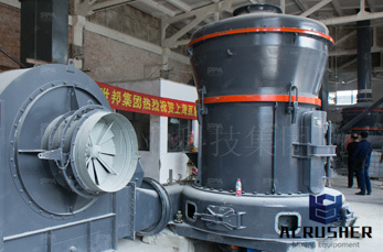
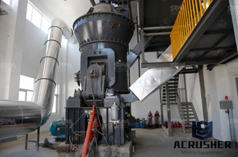
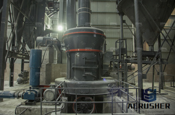
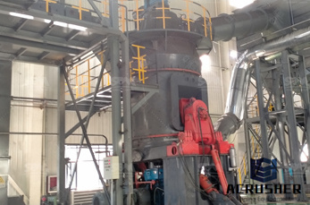
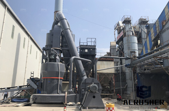
back grinding machines in semiconductor Our Purpose And Belief LM Heavy Industry is committed to provide the global customers with the firstclass products and superior service, striving to maximize and optimize the interests and values of the customers, and build bright future with high quality.
Back grinding is a process that removes silicon from the back surface of a wafer. Silicon Valley Microelectronics provides grinding on our own substrates or on customer supplied wafers. We process bare and device patterned wafers with high yield and offer wafer thinning to customer specifications. SVM Wafer Back Grinding Capabilities:
GDSI, Grinding and Dicing Services complete resource for Silicon Wafers Processing includes Probing, Bumping, Grinding, Polishing in San Jose, California. Back Grinding Services by Silicon Valley Microelectronics, Inc. (SVM). Back grinding is a process that removes silicon from the back surface of a wafer.
POREX ® Tubular Membrane Filter (TMF)™ Applied in Die Saw Wastewater Reclaim System for a Microelectronics Company in Shenzhen, China. Introduction. Die sawing and backgrinding are processes which are used to cut large silica wafers into smaller discs. After either of these processes, the wafer chips must be rinsed with Ultrapure Water (UPW) to remove fine silica particles and any other ...
Wafer Backgrind Wafer Backgrind is the process of grinding the backside of the wafer to the correct wafer thickness prior to assembly. It is also referred to as ''wafer thinning.'' Wafer backgrinding has not always been necessary, but the drive to make packages thinner and thinner has made it indispensable.
Established in 2008, DSK Technologies Pte Ltd is a youthful, dynamic and fastgrowing company. Dealing in Semiconductor materials, our business presence can be found in most parts of SouthEast Asia. Our mission is to establish DSK as the preferred Business Partner and OneStop Solution Sourcing Agent for our customers and principles.
Wafer dicing is the process by which individual silicon chips (die) are separated from each other on the wafer. The dicing process is accomplished by mechanically sawing the wafer in the extra areas between the die (often referred to as either dicing streets or scribe lines). To facilitate the sawing of the wafer, backside support [.]
Specialised in distribution, manufacturing and provisions of engineering services of inspection, test, measuring, analytical automated handling equipment.
QuikPak, originally founded in 1994 as SPT, was purchased by Delphon Industries in 2000. For the last 15 years, QuikPak has provided fast turn IC Packaging, Assembly, Prototype and Wafer Processing Services to a wide variety of Semiconductor and Electronics Companies, as well as major Military and Aerospace institutions.
Wafer Thinning. There are four primary ways to thin wafers, (1) mechanical grinding, (2) chemical mechanical planarization, (3) wet etching and (4) atmospheric downstream plasma dry chemical etching (ADP DCE).There are two groups that make up the four wafer thinning techniques: grinding .
Wafer Level Packing services, Pac Tech Asia provides a complete turnkey solution especially for PowerMOSFET products, including front metallization (Eless NiAu/ NiPdAu plating), back grinding, back metallization, dicing and die sorting. Wafer Thinning and Backmetal Specifications Wafer Thinning Wafer
In order to meet industry demands for turnkey WLCSP products, TFAMD has offered the service from Wafer Probing and Wafer Back grind as well. TFAMD use fullyautomated wafer back grinding equipment to achieve high level of quality for post grind wafer. The process includes wafer backgrinding, die singulation, AOI and packing in tape Reel.
13 hours ago· Press release KD Market Insights Wafer Backgrinding Tape Market Volume Analysis, Segments, Value Share and Key Trends published on
Back Grinding Wheel. Ceramic Capillaries. Ceramic Parts. CMP Pad Conditioner. Copper Wire. Dummy Wafer. ... Plant Engineering Services. Refurbished OEM Equipment. ... Jalan Juruukur U1/19, Hicom Glenmarie Industrial Park, 40150 Shah Alam, Selangor, Malaysia ...
Wafer Back Grinding Tapes. ... Wafers requiring grinding and thinning to 50 microns needs high performance adhesion and yet easily release on demand either by UV or heat curing. AIT wafer and substrate grinding and thinning temporary bonding adhesive tapes are made in the United States with Company Service Centers in China and USA. The high ...
WhatsApp)